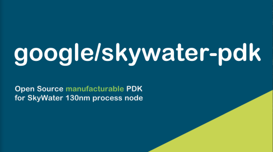
Google supports project to open source 'PDK' necessary for semiconductor chip design

Manufacturers of semiconductor products, such as CPU, you also if you have a production line in-house, but as of AMD
GitHub-google/skywater-pdk: Open source process design kit for usage with SkyWater Technology Foundry's 130nm node.
https://github.com/google/skywater-pdk
Produce your own physical chips. For free. In the Open.
https://fossi-foundation.org/2020/06/30/skywater-pdk
If you wanna make your own open-source chip, just Google it. Literally.Web giant says it'll fab them for free • The Register
https://www.theregister.com/2020/07/03/open_chip_hardware/
google/skywater-pdk-Manufacturable Open Source 130nm PDK-Google Slides
https://docs.google.com/presentation/d/e/2PACX-1vRtwZPc8ykkkgtUkHkoJZrP9jKOo3FYdKqbg-So0ic6_kx7ha1vHnxrWmuxWkTc9GfC8xl0TfEpMLwK/pub
Manufacturers of semiconductors generally purchase development kits called '
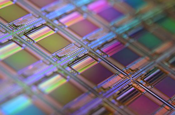
Speaking of open source projects in the semiconductor field, ' RISC-V ' is famous, but the open source PDK did not exist until now. In addition, the PDKs provided by semiconductor foundries are known to be expensive. However, the situation has changed because Google and semiconductor foundry ' SkyWater ' have released the industry's first open source PDK. Using the following PDK that Google has released on GitHub, SkyWater's 130 nm process 'SKY130' will promote open source of the semiconductor industry if it becomes possible to design for manufacturing semiconductor chips for free Philip Wagner , director of The Free and Open Source Silicon Foundation (FOSSi), explains:
GitHub-google/skywater-pdk: Open source process design kit for usage with SkyWater Technology Foundry's 130nm node.
https://github.com/google/skywater-pdk
In addition, Google has also invested in semiconductor company efabless . efabless plans to provide a free 'shuttle service' called Multi-project wafer (MPW) , which prototypes chips using a technology that mixes multiple circuits on a single wafer. This project covers all open source chip designs and is expected to serve 40 projects in November 2020.
At the time of writing the article, SkyWater's PDK for SKY130 is in alpha version, and features will be added in the future. Wagner says the open source of PDK is a dream project that can solve the big challenges that FOSSi has been addressing over the years.
Related Posts: