The resolution of the electron microscope reaches 0.39 angstroms and the world record is updated
An electron microscope that obtains an enlarged image by irradiating an object with an electron beam can see very small electron microscopes. As of 2018, world record of resolution in electron microscope was irradiated with high power electron beam of 300 k eV "0.5 Angstrom (0.05 nanometer)" which is realized with an electron microscope to be used. David Muller's team, a professor of Applied Physics at Cornell University, has succeeded in developing a technology that achieves 0.39 Angstrom (0.039 nanometer) resolution over the previous world record. Moreover, this technology can be realized with an electron microscope that irradiates a low power electron beam of 80 keV.
Electron ptychography of 2D materials to deep sub-ångström resolution | Nature
https://www.nature.com/articles/s41586-018-0298-5
A record-breaking microscope
https://www.nature.com/articles/d41586-018-05711-y
Electron microscope detector achieveves record resolution | Cornell Chronicle
http://news.cornell.edu/stories/2018/07/electron-microscope-detector-achieves-record-resolution
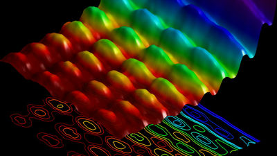
When you capture an image using an electron microscope, the image may inevitably become distorted or blurred. In order to correct this aberration, a method to clear the image by placing a correction lens has been taken so far.
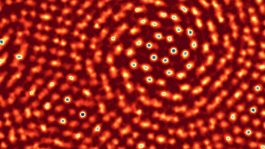
Mr. Muller's research team has investigated ways to enlarge the image more than ever and eliminate this "correction lens" and to see how to display it more clearly. Muller and others devised a method combining EMPAD of electron detector and technology called tycorography which was used in X-ray microscope . As a result, the research team succeeded in acquiring a high resolution image of 0.39 angstrom (0.039 nanometer) with an electron microscope emitting an electron beam of low power of 80 keV.
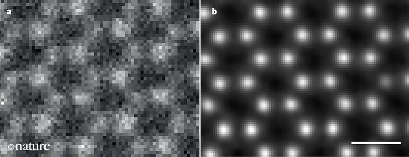
The research team photographed molybdenum sulfide (MoS 2 ) with a conventional electron microscope of 80 keV and an electron microscope using Muller's technology, in order to show to what extent the image looks clear when using the technology actually developed It is. When comparing the two images, it is clear that the method taken by Mr. Muller et al. (Right) is sharper as compared with the one photographed with the conventional electron microscope (0.98 Å) (0.098 nanometer) You can see that it is reflected.
The technology developed by Mr. Muller's research team can handle images that are susceptible to damage by electron beams because it can acquire images with high resolution with an electron microscope that irradiates low power electron beams. For this reason, it is expected to play an active part in investigating materials that have been difficult to handle with the electron microscope so far.
Related Posts:


in Science, Posted by darkhorse_log