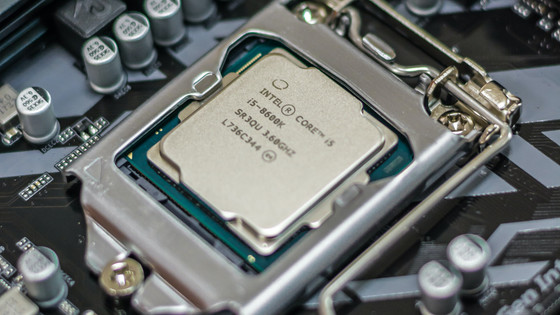
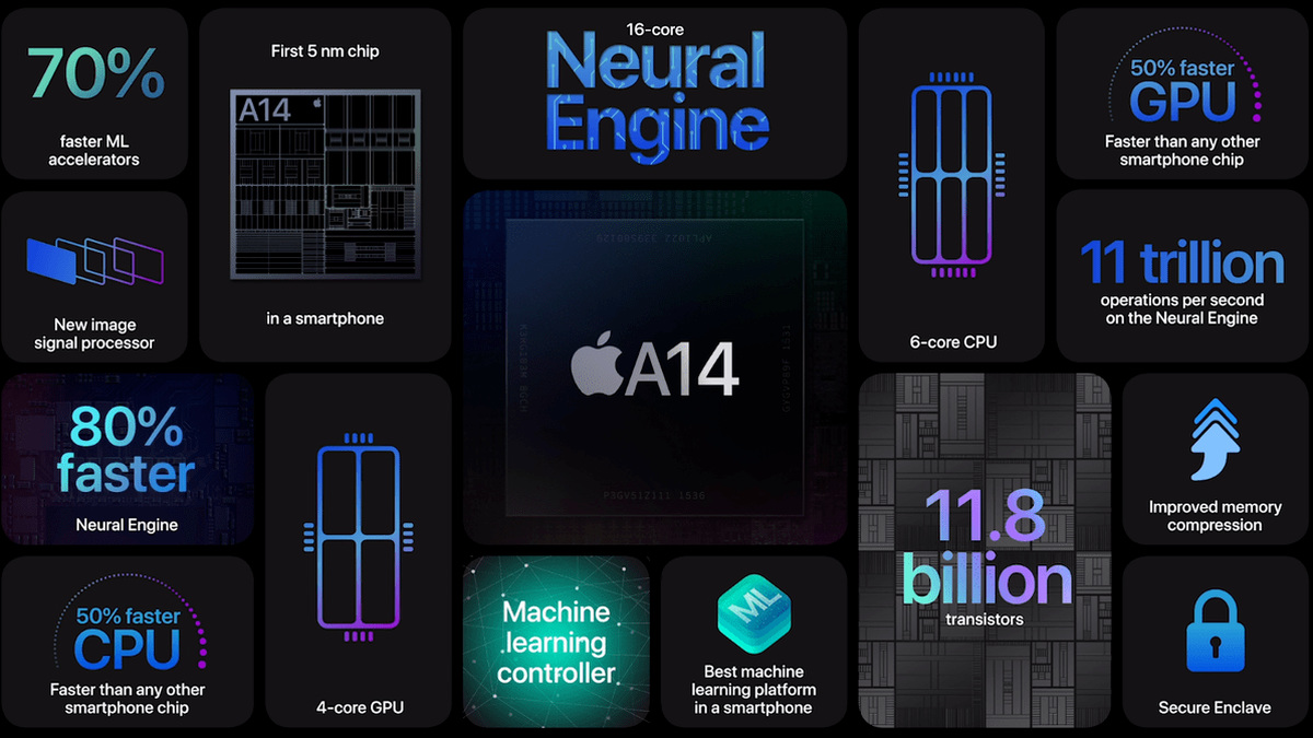
The evolution of the Apple A14 Bionic chip on the iPhone 12 hasn't come to the forefront of TSMC's 5nm process.
Apple's A14 Packs 134 Million Transistors / mm², but Falls Short of TSMC's Density Claims – SemiAnalysis
https://semianalysis.com/apples-a14-packs-134-million-transistors-mm2-but-falls-far-short-of-tsmcs-density-claims/
As the name implies, the number of transistors is the 'number of transistors on the chip', and the number of transistors per 1 mm 2 is the 'transistor density'. In addition, among SoCs, the transistor density of only logic circuits is the 'logic density', and the increase in logic density is the most obvious representation of the evolution of process nodes, which is the chip manufacturing method.
The table below summarizes the process nodes adopted from Apple's original SoCs A10 to A14, the number of transistors, the transistor density, and the logic density of each process node.
| Apple SoC | ||||||
| SoC | Process node | Number of transistors | SoC area (mm ^ 2) | SoC transistor density (Number of transistors / mm ^ 2) | Process node logic density (By Wikichip ) | Logic density ratio of transistor density |
| A10 | TSMC N12 | 3.3 billion | 125.00 | 26.4 million | 28.8 million | 91.41% |
| A11 | TSMC N10 | 4.3 billion | 87.66 | 49.05 million | 52.51 million | 93.42% |
| A12 | TSMC N7 | 6.9 billion | 83.27 | 82.86 million | 91.2 million | 90.86% |
| A13 | TSMC N7 | 8.5 billion | 94.48 | 89.97 million | 91.2 million | 98.65% |
| A14 | TSMC N5 | 11.8 billion | 88.00 | 134.09 million | 171.3 million | 78.28% |
Apple is appealing the number of transistors when talking about the performance of its own SoC. The transistor density produced from this number of transistors has achieved more than 90% of the logic density of the process node adopted.
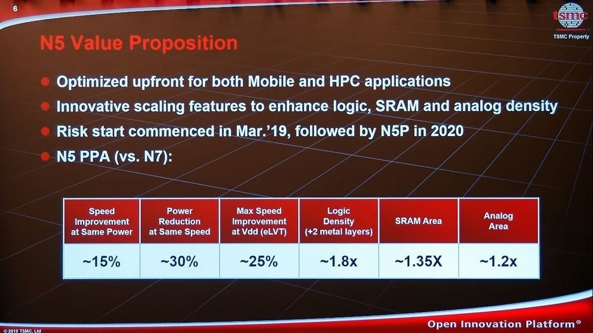
However, with the A14, the achievement rate is 78.28%. In addition, TSMC claims that the logic density of the 5nm process 'N5' will be more than 1.8 times that of the 7nm process 'N7', but the transistor density of the A14 Bionic is 1.49 compared to the previous generation A13 Bionic. Double. From this, it can be seen that the evolution rate of transistor density cannot keep up with the evolution rate of logic density.
SemiAnalysis states that the transistor density of the A14 Bionic is not keeping up with the logic density of TSMC, not because of TSMC or Apple's failure, but because of the delay in
SRAM is widely used throughout the processor, from
SemiAnalysis pointed out that the logic density of N5 was 1.8 times higher than that of N7, while the SRAM density was 1.35 times, and TSMC's N5 stated that SRAM miniaturization was slowing down. I will. Of course, major semiconductor manufacturers such as TSMC and Samsung are developing technology to solve the problem of slowing the miniaturization of SRAM, and in August 2020 Samsung will stack logic and SRAM vertically3 We are announcing dimensional structure mounting technology.
Samsung, 7nm EUV process with logic and SRAM 3D IC | Nikkei Crosstech (xTECH)
https://xtech.nikkei.com/news/
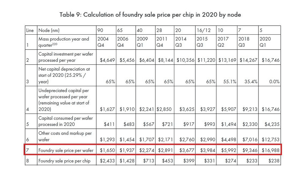
SemiAnalysis claims that even if the problem of SRAM miniaturization is solved, the improvement in cost performance is definitely slowing down. With the evolution of process nodes, the price of semiconductor wafers is rising, and the cost per N7 and N5 transistors is about the same.
Related Posts: