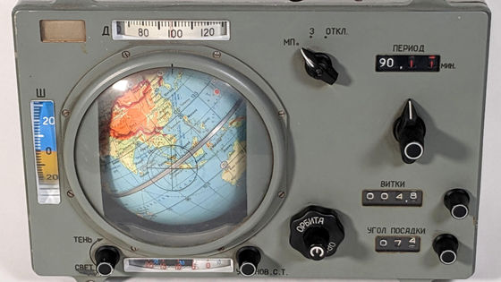
What was the design of the clock of the former Soviet rocket 'Soyuz'?
During the Cold War period after World War II, the United States, which represented the western nations, and the Soviet Union, which were the eastern countries, had a fierce competition for space development. Engineer
Looking inside a vintage Soviet TTL logic integrated circuit
http://www.righto.com/2020/03/looking-inside-vintage-soviet-ttl-logic.html
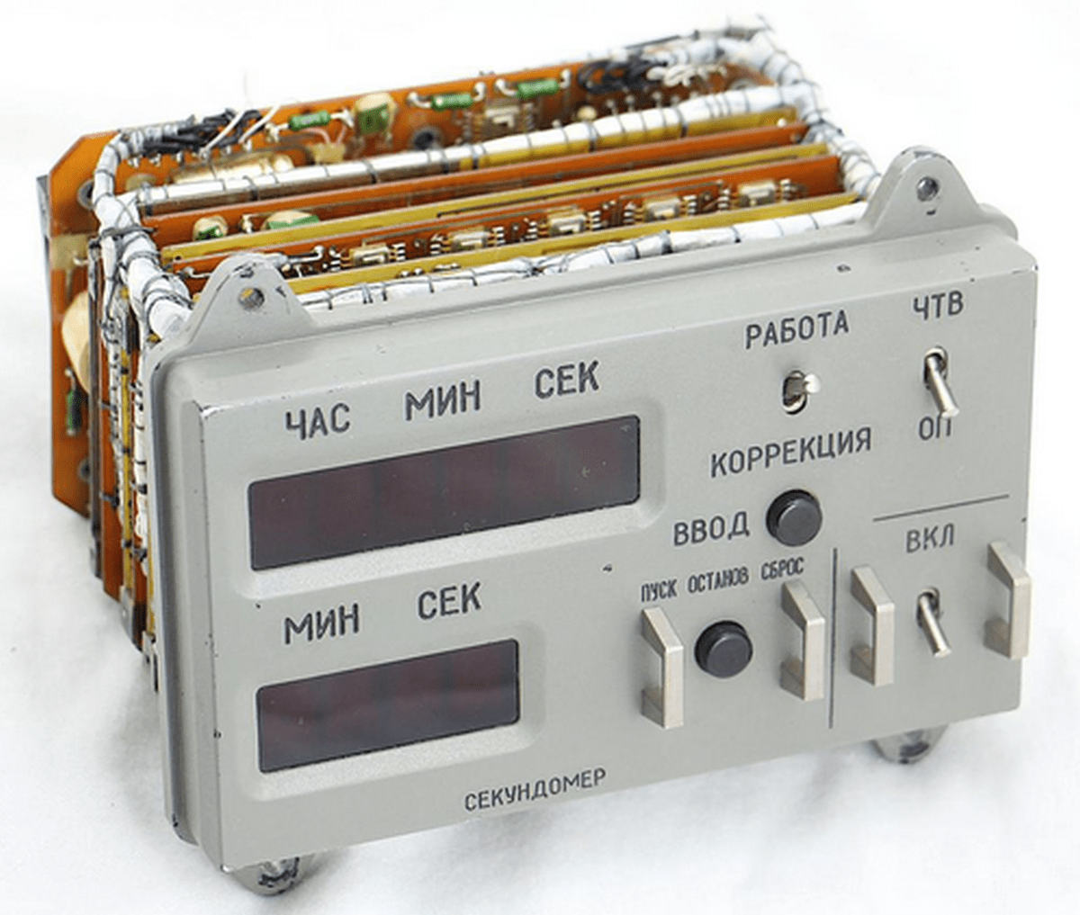
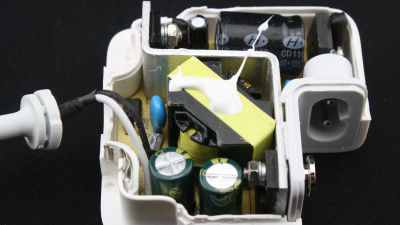
This is the image of the watch that was actually removed from the Soyuz watch. The upper LED display shows the time, and the lower LED display shows a stopwatch. Ken says the watch has a very complex structure for its function.
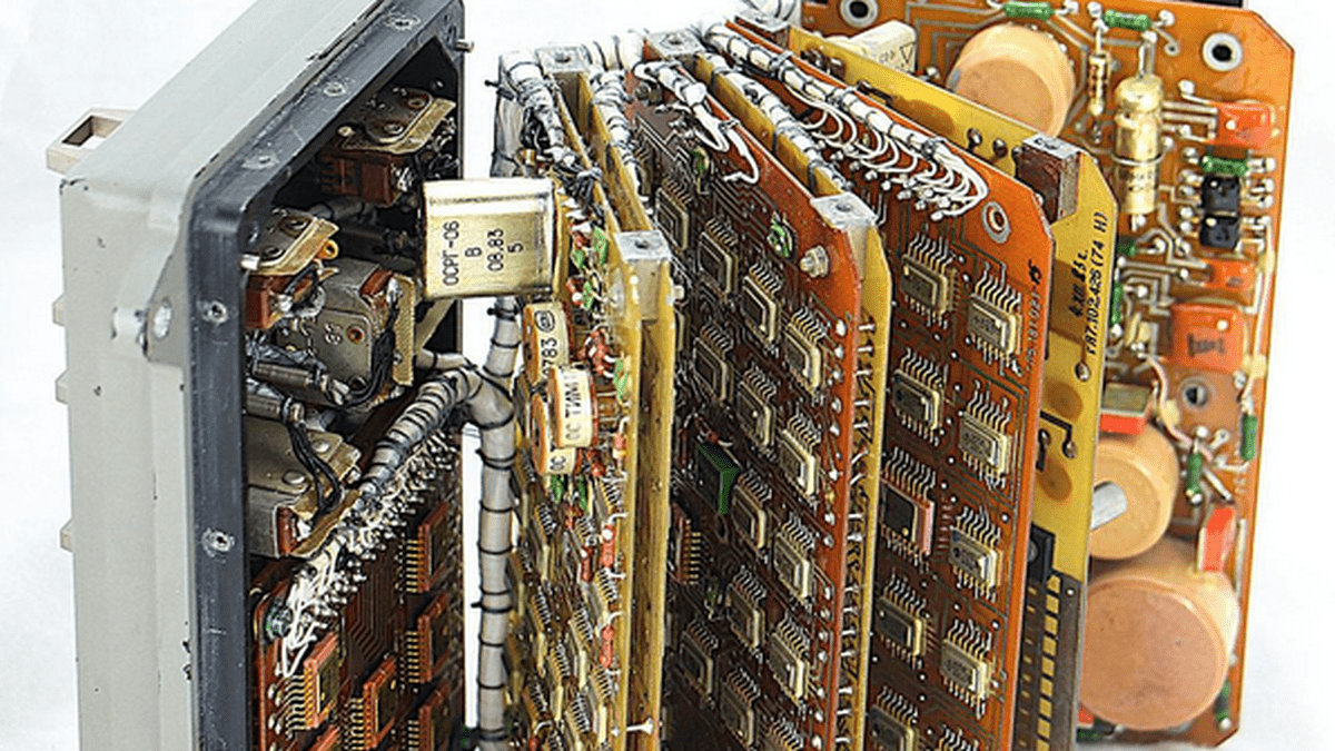
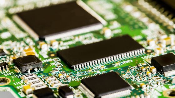
I opened the clock board. Most
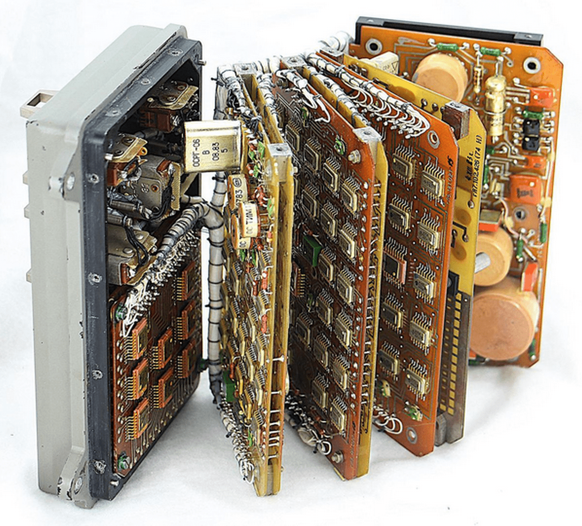
Clock chips use
When the silicon die is enlarged with a microscope, it looks like this: the pink and purple parts are silicon, and the white parts are wires.
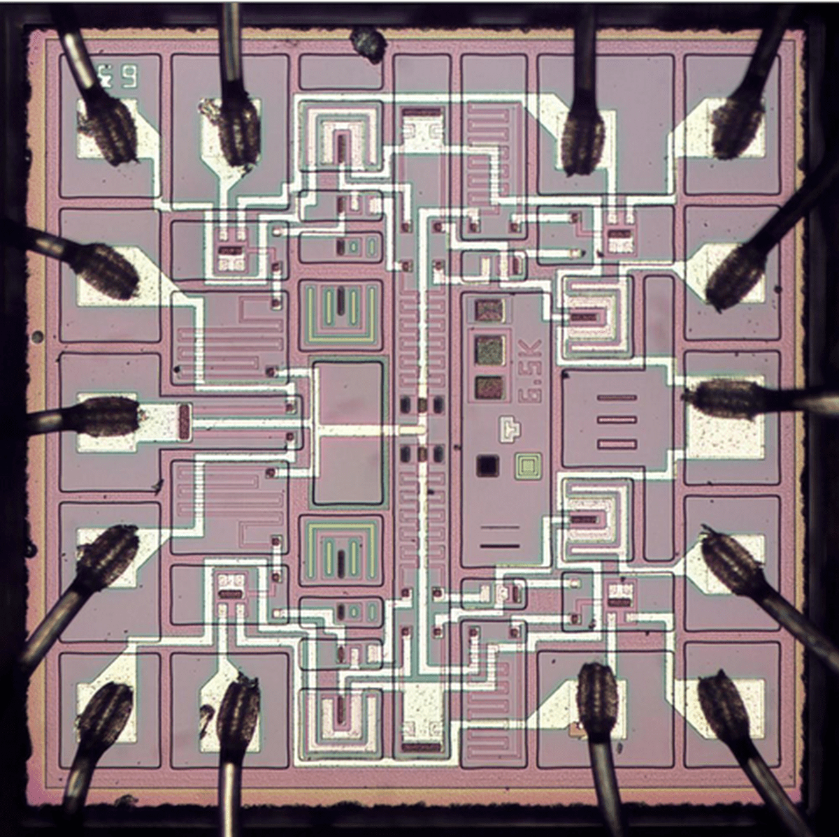
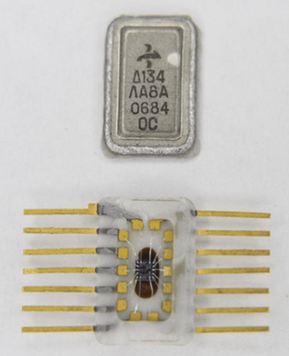
The chip is called '134ЛА8' and was manufactured in 1984. At the time this chip was developed, the Soviet Union was behind the United States in developing integrated circuits for about nine years. As a result, the Soviet Union often copied western integrated circuits, but Ken speculates that the Soviet Union designed 134ЛА8 independently.
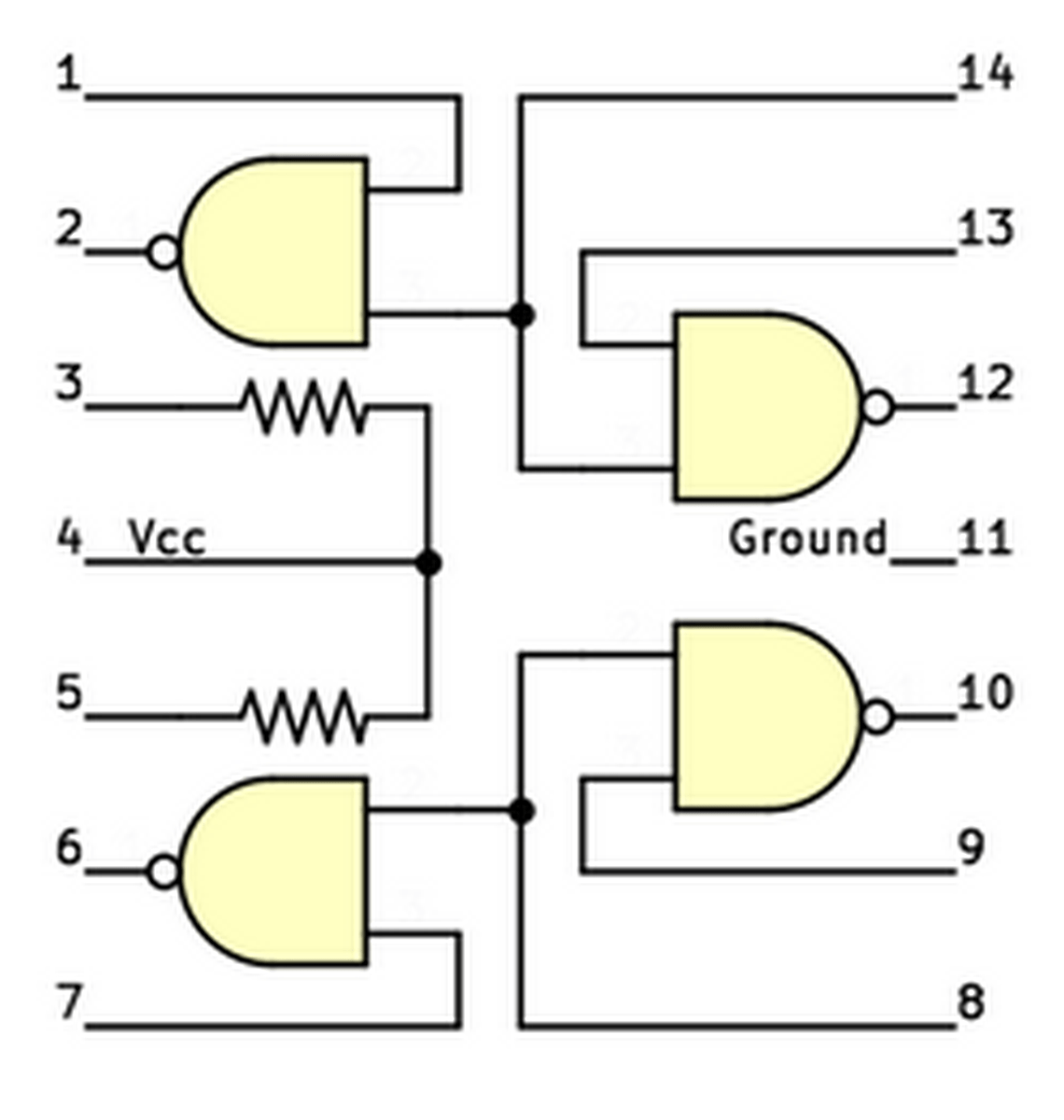
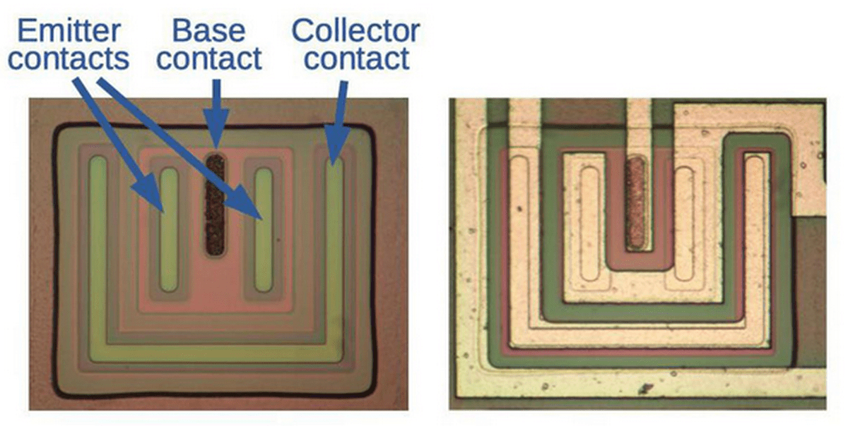
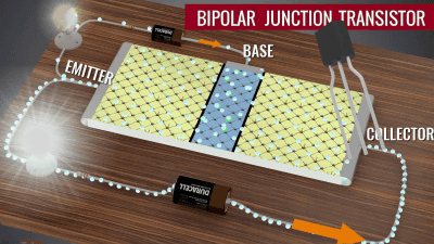
The 134ЛА8 has four open collector NAND gates. An open collector is a type of operating a potential by using a transistor as a switch. A transistor is made up of three terminals called a 'base', 'collector' and 'emitter', and controls the current between the collector and the emitter through the current flowing through the base.In general, the transistor is pulled to stabilize the output. Use up resistor at the same time. This chip has one circuit for the crystal oscillator and two circuits for conversion.
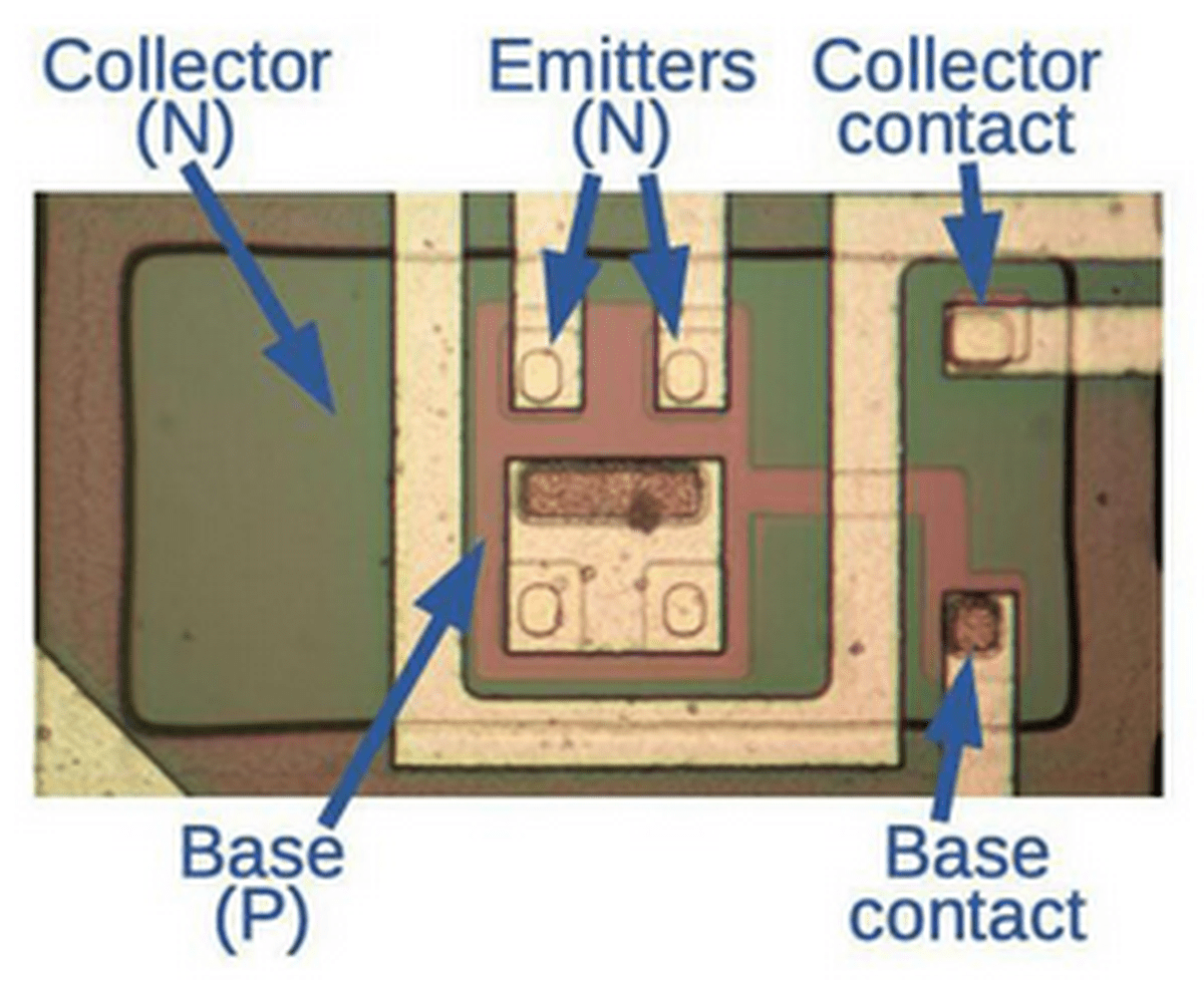
If you enlarge the silicon die with a microscope, you can see its composition. Semiconductors come in two
134ЛА8 adopts
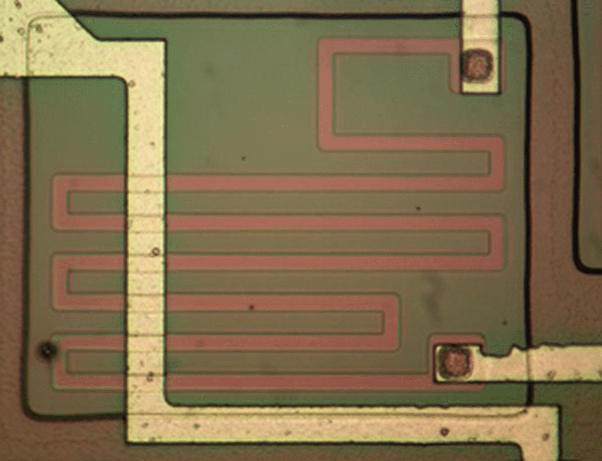
The transistor for external output generates an external signal, so much higher current flows than other transistors. As a result, Ken says, the size is larger than other transistors. The image shows a 134ЛА8 external output transistor, which has larger emitter and collector terminals than the previous transistor.
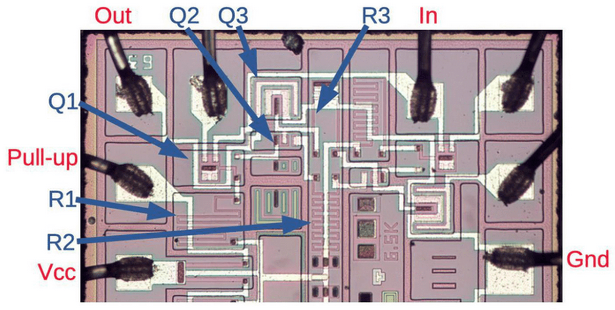
This is a circuit diagram showing one of the implemented NAND circuits. If at least one of the inputs is 0, transistor Q3 turns off. At this time, the current on the output side is in an “open” state where there is nowhere to go and outputs 1 at the open collector. If both inputs are 1, the switches of transistors Q1, Q2, and Q3 are turned on, and the current on the output side flows to GND, so the circuit outputs 0 at the open collector.

It looks like this when photographing the actual circuit with a microscope. A NAND circuit is implemented by making good use of transistors.
Ken said, 'This Soviet chip is simple enough to easily trace the circuit. The latest chips today contain billions of transistors and have so many features. You cannot visually understand the contents of the chip. '
Related Posts:

in Hardware, Posted by darkhorse_log