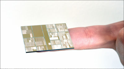
Technology to irradiate nanoscale IC chips with X-rays and analyze and investigate the inside nondestructively
By using
Three-dimensional imaging of integrated circuits with macro- to nanoscale zoom | Nature Electronics
https://www.nature.com/articles/s41928-019-0309-z
X Ray Tech Lays Chip Secrets Bare IEEE Spectrum-IEEE Spectrum
https://spectrum.ieee.org/nanoclast/semiconductors/design/xray-tech-lays-chip-secrets-bare
Although Moore's Law that 'the number of transistors in a semiconductor integrated circuit doubles every two years' is said to have entered the end in recent years, although the pace has dropped, the structure of the CPU is still miniaturized and high Continues to increase density.
by
Therefore, in order to reverse engineer the IC chip, it takes tremendous effort and time, such as removing one part at a time in nanometers and imaging a layered circuit using optical microscopy to electron microscopy thing. Also, because the IC chip is too small to be reassembled, valuable samples will be lost if reverse engineering is successful.
Meanwhile, a research team such as Gabriel Eppli, professor of physics at the Technical University of Zurich, reported in his paper that 'We have developed a new technique for analyzing the structure of IC chips using X-rays.' . Using this new technology named 'ptychographic X-ray laminography', non-destructive reverse engineering is achieved by applying X-rays emitted from synchrotrons to IC chips. You can do it.
In fact, Mr. Eppli also developed “X-ray ptychography” , a similar technology in 2017. However, due to technical limitations, the detailed structure of the latest IC chip could not be elucidated.
One of the problems that plagued Epri et al. Was the problem that when a chip was irradiated with X-rays from the front, the X-rays were absorbed and a useful diffraction pattern could not be obtained. For this reason, X-ray typography developed in the past uses a method of inferring the structure of an IC chip from how X-rays are scattered by irradiating X-rays from various angles using a 10-micrometer column. It was
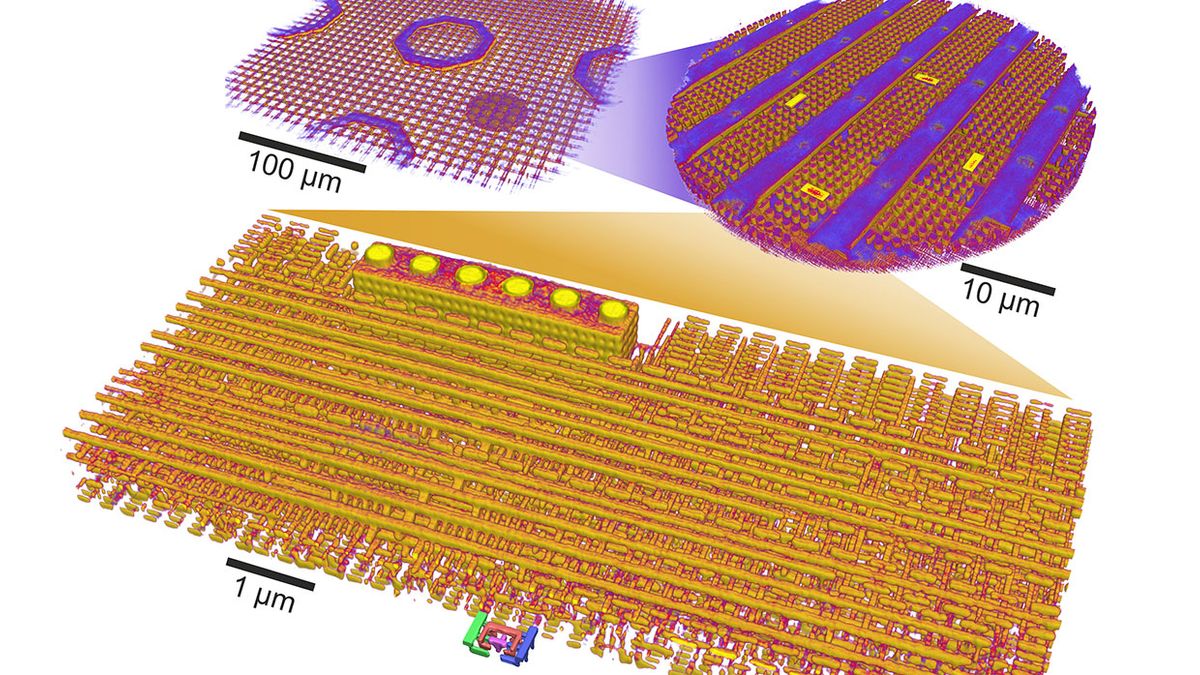
On the other hand, with this new technology, X-rays were radiated from an oblique angle of 61 degrees, and the conventional problem was solved by a technique that balances the accuracy lost with the information lost by X absorption. Scanning IC chips using new technology first scans an area of 300 micrometers x 300 micrometers on a side over 30 hours in low resolution mode. After discovering the heart of the IC chip, this time, the region of 40 micrometers in diameter is analyzed over 60 hours in high resolution mode. X-rays have a very short wavelength and are more like photons than electromagnetic waves, so a special camera called a
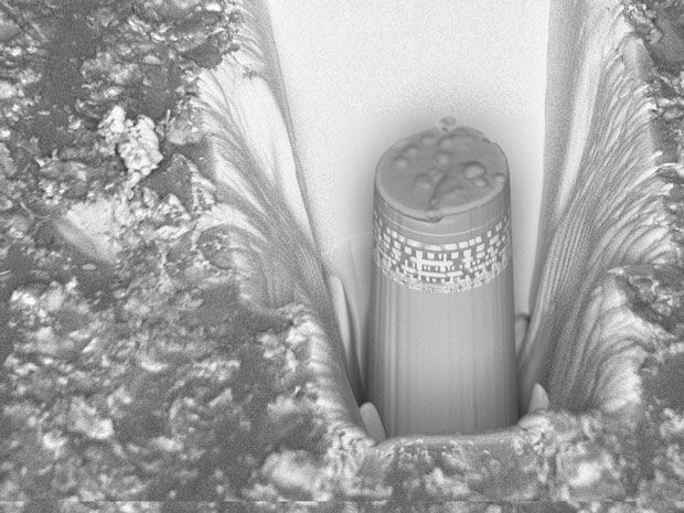
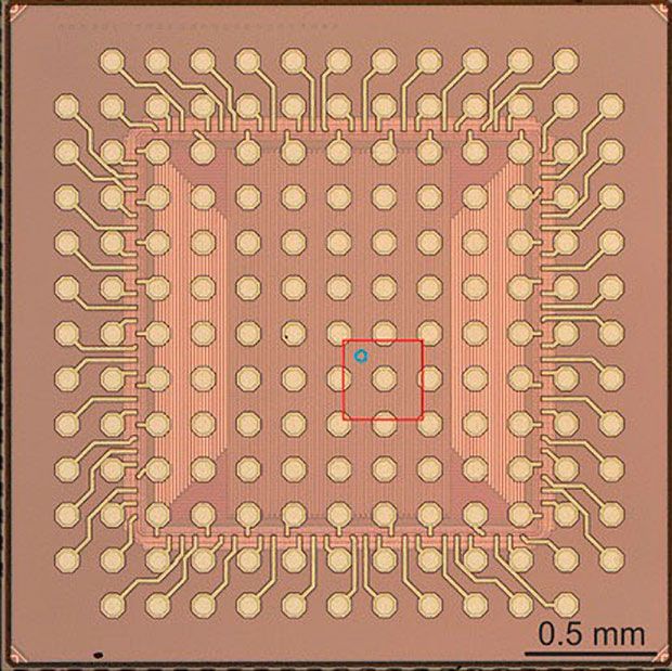
The following image is an image of analysis of an IC chip by typographic X-ray tomography. The red frame represents an area of 300 micrometers x 300 micrometers, and the blue circle represents an area of 40 micrometers in diameter.
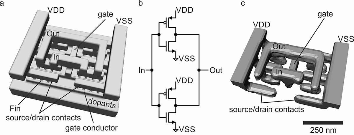
By creating a 3D model based on the data obtained in this way, he succeeded in identifying the circuit structure of a
By using this technology, it is possible not only to inspect whether the manufactured IC chip has the structure as designed, but also to reverse engineer IC chips with unknown structures.
“Currently, it takes 90 hours to diffract IC chips, but if you can irradiate with a sufficient flow rate of X-rays from the latest synchrotron, such as the MAX IV laboratory in Sweden, 'We will be able to reduce the inspection time to less than one hour in the near future,' he said, and expressed his view that it will be possible to perform much quicker analysis in the future.
In addition, Mr. Epri said, “I have already been consulted by the US national security authorities,” and revealed that it is not only used in the industrial field but also in security fields such as spy chip detection . It was.
Related Posts: