NVIDIA is accused of "VRAM 3.5 GB problem" of GeForce GTX 970
GPU released in 2014 by American semiconductor manufacturer NVIDIA "GeForce GTX 970"It was raised a class action in North Carolina State, assuming that the specification of the hardware was misrepresented.
Nvidia lawsuit over GTX 970
http://ja.scribd.com/doc/256406451/Nvidia-lawsuit-over-GTX-970
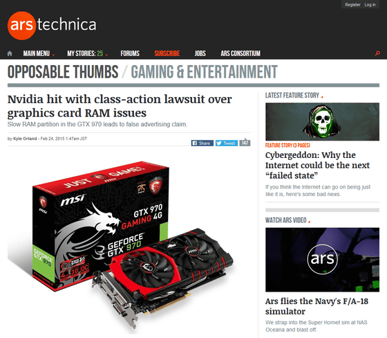
Nvidia hit with class-action lawsuit over graphics card RAM issues | Ars Technica
http://arstechnica.com/gaming/2015/02/nvidia-hit-with-class-action-lawsuit-over-graphics-card-ram-issues/
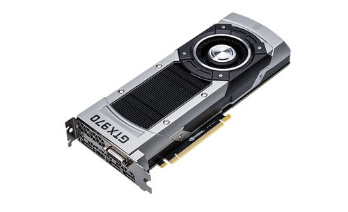
It is the graphic board (graphic card, video card) that exclusively performs the work of inputting and outputting the image as a signal by the PC, and the processor unit on this board is called GPU. NVIDIA sells GPUs in several brands including "GeForce" for gaming, "Quadro" for professionals, "Tesla" for high performance, etc. In September 2014, GPU for gaming "GeForce GTX 970 We released the.
GTX 970 is a next generation architectureMaxwellIt has a built-in new core using, power saving, powerful, can be purchased relatively cheaply, and it made a big hit worldwide.
However, it is discovered by writing in GeForce 's forum that there is a problem with GTX 970 since 2015.
GTX 970 3.5 GB Vram Issue - GeForce Forums
https://forums.geforce.com/default/topic/803518/geforce-900-series/gtx-970-3-5gb-vram-issue/
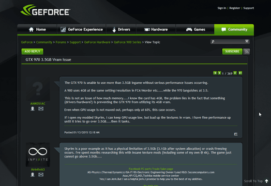
In the thread named "GTX 970 3.5 GV Vram Issue" created in the forum, "Written that the GTX 970 can only use 3.5 GB of VRAM and has serious problems in its performance" It was. According to the user who wrote it, these problems did not occur in "GTX 980" which was released as the same VRAM 4 GB model at the same time. "Skyrim'sMODIt will show off amazing performance up to 3.5 GB when opened, but it will be useless if it is more than that. "
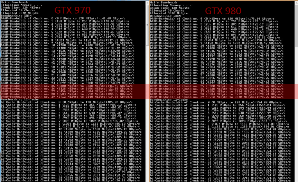
Since not only a single user but also many users reported problems on "VRAM of GTX 970", many media started to verify VRAM of GTX 970, and as shown in the image belowPublish benchmark resultsI will start. In the VRAM of GTX 970, you can see that the speed is dramatically slowed down after 3200 MiB by looking at the value of the red part.
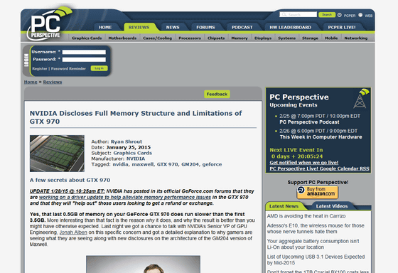
Meanwhile, John Alben, NVIDIA 's GPU development department, explained to the media about "VRAM 3.5 GB problem of GTX 970" and described it in the "Review Words Guide" distributed for reporters reviewing The specification table which I was doing was wrong, and I released the specification of the accurate GTX 970.
NVIDIA Discloses Full Memory Structure and Limitations of GTX 970 | PC Perspective
http://www.pcper.com/reviews/Graphics-Cards/NVIDIA-Discloses-Full-Memory-Structure-and-Limitations-GTX-970
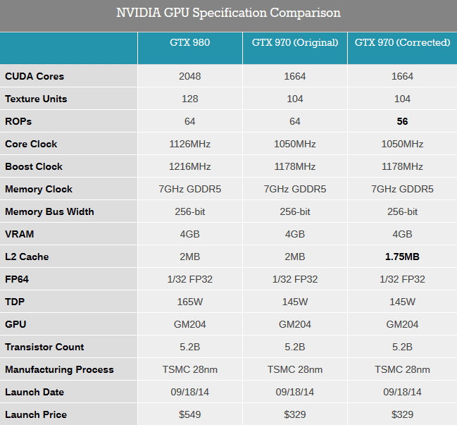
"Corrected" published by NVIDIA is written in "GTX 970 (Corrected)" in the table below, and the one written in "GTX 970 (Original)" is the GTX 970 published by NVIDIA at the time of release spec. Although there is almost no big difference, "ROPs" which is a dedicated unit for writing the color of each pixel in the VRAM changes from 64 to 56, "L2 cache"Has decreased from 2 MB to 1.75 MB.
Although it was GTX 980 and GTX 970 which were released at the same time, the problem was only in GTX 970, the reason being the difference between the two L2 caches. In GTX 970, 13 computing devices (SM) are enabled, and there are 128 CUDA cores in each SM, so when they are all combined, it will be 1664 CUDA cores. And, as you can see in the figure below, all 13 SMs are connected to parts that play a role like a switch connecting SM and L2 cache called crossbar. In the case of GTX 980, there are 8 L2 cache (2 MB), but in GTX 970 only one out of 8 is invalidated and if the seventh L2 cache does not exchange 2 pieces of information It has gone wrong.
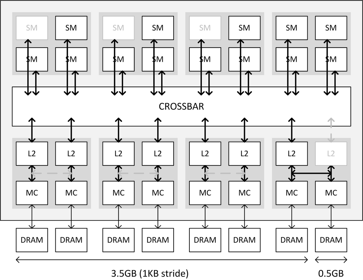
As the seventh port is required to transmit twice as much information, the performance will be extremely lowered, so NVIDIA has two sections of DRAM 7 (3.5 GB) and one (0.5 GB) It will split and create a special configuration of fast 3.5 GB VRAM and slow 0.5 GB VRAM. NVIDIA accesses 1-2-3-4-5-6-7 and DRAMA in turn from the crossbar so that the 3.5 GB VRAM takes precedence, and then does not access the 8th DRAM and again It seems that the bandwidth was balanced by designing it to access DRAM applied to 3.5 GB VRAM. However, if you use more than 3.5 GB of memory, performance has declined extremely.
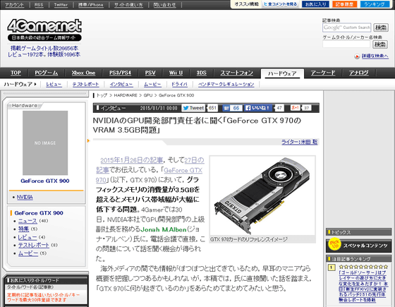
Japan's 4 Gamer is also asking Mr. Alben to ask questions about GTX 970 using a video phone and is drawing more detailed information on the composition of the GTX 970.
"VRAM 3.5 GB problem of GeForce GTX 970" asked NVIDIA's GPU development department manager - 4Gamer.net
http://www.4gamer.net/games/274/G027467/20150130109/
NVIDIA noticed a mistake in the specification table described in the "Review Words Guide" distributed for the media when releasing the GTX 970, about four months passed since the launch, and it was noticed after complaints were flooded by many users is. In addition, NVIDIA does not disclose detailed specifications of GTX 970 on the official website, and explains, "The material distributed to the media has spread through the report". The plaintiffs who filed a class action against it commented that "NVIDIA has carried out a plan to cheat consumers globally".
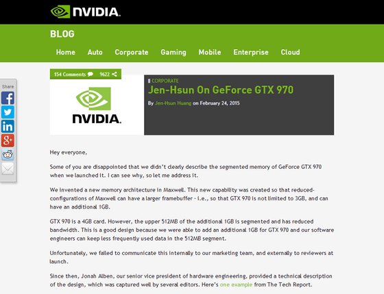
In addition, NVIDIA's CEO Jen Seung Huan officially opens a description.
Jen-Hsun On GeForce GTX 970 | The Official NVIDIA Blog
http://blogs.nvidia.com/blog/2015/02/24/gtx-970/
· 2016/08/01 10:10 postscript
This class action was settled by NVIDIA paying GTX 970 purchasers $ 30 per person (about 3000 yen).
Show_temp.pl - 2. pdf
(PDF file)https://cdn.arstechnica.net/wp-content/uploads/2016/07/show_temp.pl-2.pdf
Nvidia offers $ 30 to GTX 970 customers in class action lawsuit over RAM | Ars Technica
http://arstechnica.com/tech-policy/2016/07/nvidia-offers-30-to-gtx-970-customers-in-class-action-lawsuit-over-ram/
Related Posts:

in Hardware, Posted by logu_ii