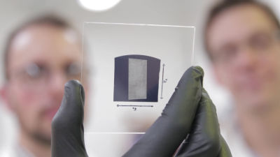
Succeeded in making the world's first "carbon nanotube computer", actual operation also
ByGeoff Hutchison
While it is said that the evolution of modern computers consisting of silicon wafers and transistors is reaching the limit, the research team at Stanford University creates "Carbon Nanotube Computer" which is one of the next generation computer technologies and calculates for the first time in the world We took a new step towards realization.
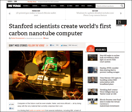
Stanford scientists create world first carbon nanotube computer | The Verge
http://www.theverge.com/2013/9/25/4769658/stanford-scientists-create-worlds-first-carbon-nanotube-computer
Successfully making this carbon nanotube computer (CNT computer) is a scientific team of Stanford University in the United States. Max Shulaker, one of the research teams, said in a paper published in "Nature" that "This is the most complicated electric circuit using CNT at the moment. Various research results have been published so far However, no one was able to answer about whether it really is usable, "he says about the significance of this achievement.
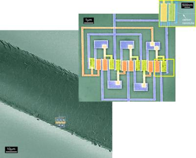
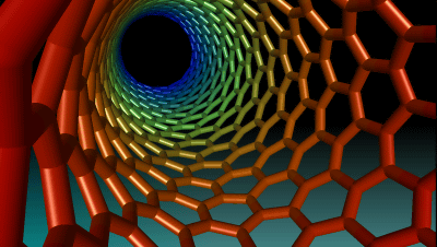
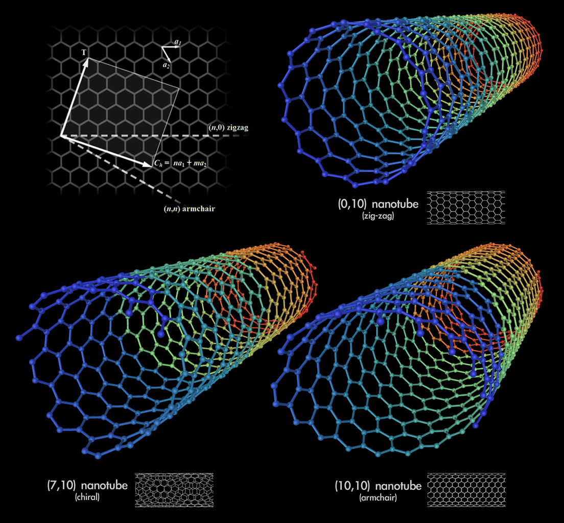
"Carbon nanotube" is a very fine structure composed of carbon atoms. It has a structure like rolled sheet of carbon atoms bonded in a network shape into a cylindrical shape, and its size is 0.4 to 50 nm (nanometer) as the name of "nano" shows. Because the size of one atom is 0.1 nm, it is just a structure of "atomic level".
Currently, almost all computers are made of silicon chips that make up transistor circuits on silicon wafers, but "the number of transistors on an integrated circuit doubles every 18 months (= 1.5 years) It is calledMoore's lawAs a result of continuing to evolve along, it is believed that the limit is approaching its evolution. Meanwhile, this CNT computer gathers expectations as a processor with high conductivity, high speed switching performance and saving size, realizing both high speed processing and high efficiency. However, to realize that, there were two problems of "self organization" and "selection of conductors and semiconductors".
"We had to tackle a lot of things to arrange the CNTs in thought and to ensure complete reliability," Shulaker says. "In a chip world where hundreds of millions of circuits are lined up, it is a very big problem even at" 2% fraction defective "."
BySolarWorld USA
To overcome this problem, we developed a method called "imperfection-immune design" which electrically evaporates CNTs with metallic properties (defects) at the manufacturing process stage. According to Shulaker, this method can be applied to mass production of CNT transistors in the future, "It shows that it can be compatible with silicon chip computers".
Although it is a CNT computer realized by a lot of efforts, 178 transistors currently installed are available, the possible processing is simple calculation and sort processing, and only toggling between two points. Although CNT computer technology just recently started to walk, Mr. Shulaker came in the future when this technology will be put into practical use, "the day when what is now called" Silicon Valley "is called" Carbon Valley " I think that it will come. "
ByGareth Royle
Related Posts: