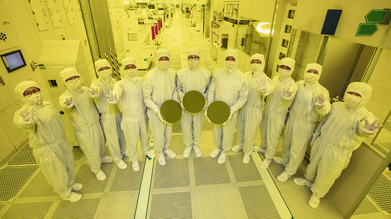
TSMC Starts Pre-Production of 5nm Process, Achieves 1.8x Transistor Density and 15% Speed Increase from 7nm Process
TSMC Ecosystem Partners Deliver Industry's First Complete Design Infrastructure for 5nm Process Technology
https://www.tsmc.com/tsmcdotcom/PRListingNewsAction.do?action=detail&language=E&newsid=THPGWQTH
Apple now available to design 5nm A-Series chips for 2020 iPhones-9to5Mac
https://9to5mac.com/20019/04/08/5nm/
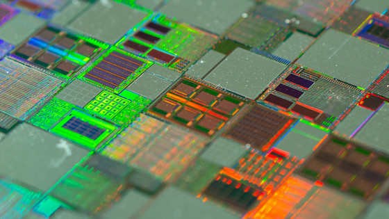
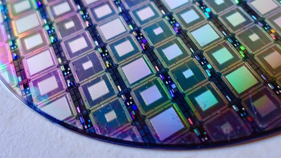
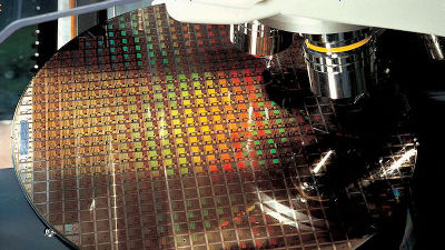
The wiring width when manufacturing semiconductor circuits on a wafer is called process rule (manufacturing process). If this minimum processing size becomes smaller, more transistors and wires can be arranged in the same area, and it is thought that semiconductor speedup can be realized. The 5 nm process that TSMC has launched to provide the design substrate is manufactured by extreme ultraviolet lithography (EUV) , and has 1.8 times the transistor density and 15% speed increase, and the memory and power optimization compared with the company's 7 nm process. It has been realized. TSMC plans to offer the 5nm process as a key target for the 5G mobile market and the AI market, which are expected to grow in the future.
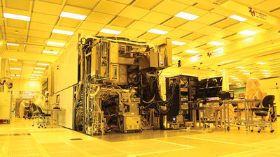
We started this time with Risk Production, in which TSMC will start production without receiving customer requests, and it will take some time before products with a 5 nm process actually become available. If Apple is outsourcing semiconductor manufacturing to TSMC, it is likely that the 2020 model iPhone will be equipped with a 5 nm process chip. In addition, TSMC aims to achieve 3 nm process in 2022.
Related Posts:


in Hardware, Posted by darkhorse_log