IBM succeeded in manufacturing 5-nm process chip, to make the world's first EUV lithography practical application
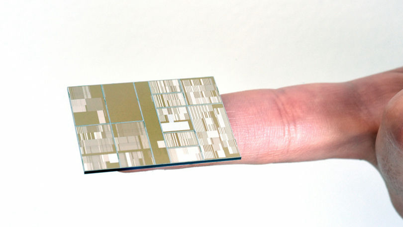
"The integration density of semiconductors doubles in 18 months"Moore's law"Is in the semiconductor manufacturing that has been whispered that no longer hold, has revealed with IBM has been successful in chip development of the world's first 5nm process. Power consumption performance is expected to dramatically improve with 5 nm process chip.
IBM unveils world's first 5 nm chip | Ars Technica UK
https://arstechnica.co.uk/gadgets/2017/06/ibm-5nm-chip/
IBM succeeded in developing by having a circuit width of 5 nmProcess ruleIn the world's first "(Extreme ultraviolet lithography (EUV:Extreme ultraviolet lithography)"Manufactured using technology. Technical cooperation is provided to IBM by GlobalFoundries and Samsung of semiconductor manufacturing.
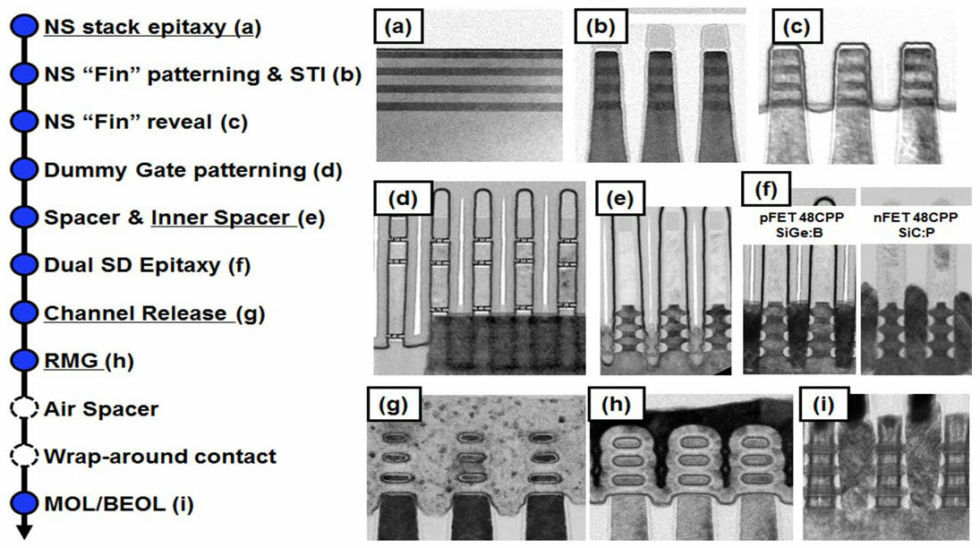
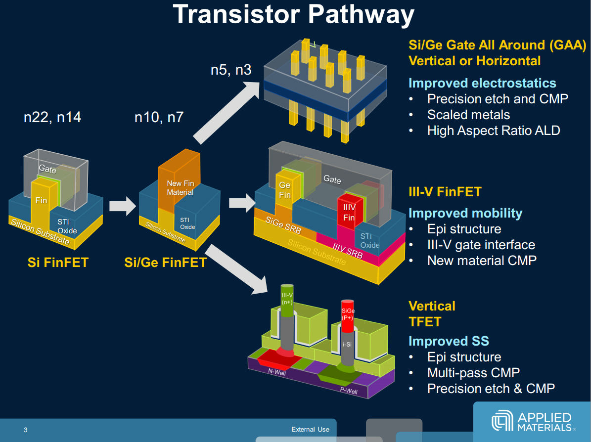
In the 5-nm process chip, it is an example that not only extreme ultraviolet lithography but also "gate-all-around (GAA)" was commercialized for the first time in the world. GAA is aimed at making it easy to control current by surrounding the nanowire with gate electrode, it can switch at high speed and compensates for shortcomings of conventional FinFET which stacks semiconductor circuits in the vertical direction. The following (a) to (i) show the manufacturing process of the 5-nm process GAAFET. In the manufacture of GAAFET, silicon (Si) and silicon germanium (SiGe) are alternately stacked, SiGe is removed by a method called "atomic layer etching" to leave a gap, and the gap is filled with a high dielectric constant film (high-k material ) And make it.
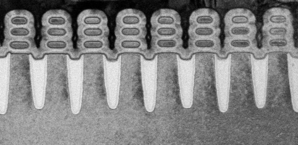
This is an enlarged view of the cross section of the completed 5-nm process GAAFET. Each transistor consists of nanosheets stacked vertically in a three-layer structure and is arranged so that the gate material surrounds them.
In the method using EUV in the manufacture of GAAFET, the process rule can be evolved to 3 nm at maximum.
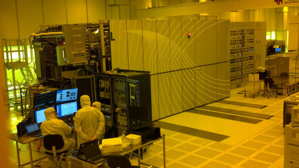
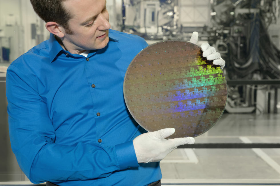
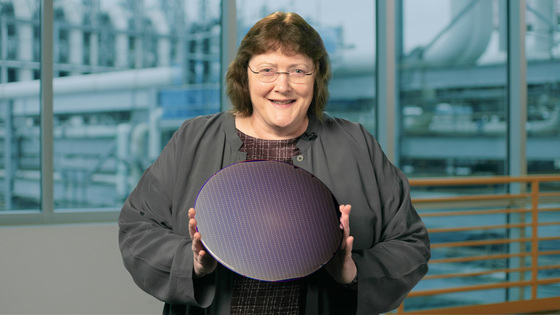
This is the world's first wafer of semiconductor chip manufactured with 5 nm process. Mr. Huming Boo, a semiconductor manufacturing manager at the IBM laboratory,EUV lithographyIs the first example used for patterning the front end. " It seems that the number of patterning steps can be reduced by using a wavelength as short as 13.5 nm in EUV, whereas the wavelength of existing immersion lithography equipment is 193 nm.
The semiconductor manufacturing technology based on EUV, which took about 10 years to put into practical use, will be put into the market in a few months. According to IBM, the 5 nm process chip achieves 40% improvement in performance and 75% reduction in power consumption with the same power compared with the 10 nm process chip currently on the market.
In semiconductor manufacturing, new technologies are often introduced in an overlapping manner with the manufacturing technology of existing products in order to lower the manufacturing cost and improve the reliability, so it is said that the 5-nm process GAAFET product will be born instantaneously I will not. As a result, Ars Technica UK points out that there is a possibility that finFETs manufactured with existing SiGe may be miniaturized to 7 nm process or 5 nm process instead of 5 nm process GAAFET.
Related Posts:


in Hardware, Posted by darkhorse_log