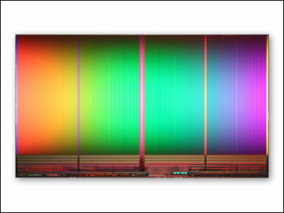
Toshiba develops NAND flash memory using state-of-the-art 43 nm process
It is said that Toshiba has announced that it has developed a high-capacity NAND type flash memory using the state-of-the-art 43 nm process at ISSCC International Society of Semiconductor currently being held in San Francisco, USA.
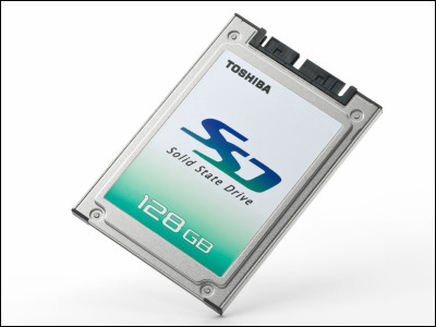
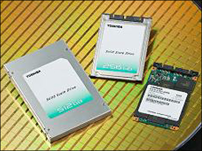
Generally, as the manufacturing process becomes smaller, there is the merit that not only manufacturing cost and power consumption will be lowered, but also more chips can be mounted on the same area, but apparently with the advent of NAND flash memory adopting this process , It seems that higher capacity and inexpensive SSD etc. will be on the market.
Details are as below.
Development of NAND type flash memory using 43 nm process
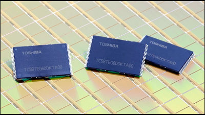
According to this release, Toshiba announced that the NAND type flash memory using the 43 nm process is a large capacity memory of 16 gigabit (2 GB) in one chip.
And by redesigning the design of the number of memory cells, peripheral circuits, power supply wiring etc., the area efficiency has been improved and the chip area has been successfully reduced by 30% compared to the same capacity product of the same 56 nm generation .
Mass production of this memory started in March and mass production of the 32 Gbit model which doubled the capacity is started even after this July.
Related Posts: